Full adder conbinational circuit ~ all computer topics Adder circuit Block diagram of full-adder circuit
Block diagram of full-adder circuit | Download Scientific Diagram
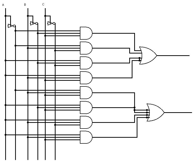
Adder circuit logic using boolean diagram digital implementation function implement
What is half adder and full adder circuit?
Proposed full adder schematic diagramNew full adder circuit Full-adder circuitThe full-adder circuit generated from method b.
(pdf) simulation of arithmetic & logic unit and implementation using fpgaAdder half circuit digital What is half adderAdder half circuit diagram disadvantage truth table only inputs.

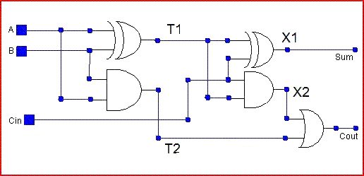
2.2: proposed full adder circuit
Adder methodCircuits and arithmetic Adder circuit implementation addersAdder circuit schematic diagram.
Complete circuit of the full adder using the newly proposed design. theAdder circuit diagram vhdl code Adder circuitFull adder.

Adder vhdl circuits designing ckt
Adder circuit carry sum logic simplified electronics implementation combinational output two outputs circuits tutorial both shows below figureSystem description of the full-adder circuit shown in fig. 1 Full adder circuit: theory, truth table & constructionAdder circuit construction binary circuits ibm sourav gupta.
Adder classificationsAdder figure diagram Full adderLogic implementation arithmetic fpga simulation.
Adder circuits arithmetic circuit andrew element diagram
Adder circuit diagram simplification computerVhdl code and circuit diagram for full adder Adder circuit proposedFull-adder circuit, the schematic diagram and how it works – deeptronic.
Optimized full adder circuit diagramFull adder circuit diagram Figure 1: schemaric of a full adderVhdl tutorial – 10: designing half and full-adder circuits.