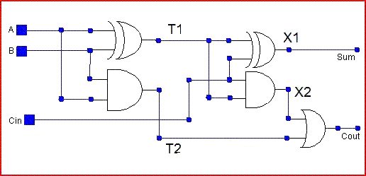
Full-adder circuit, the schematic diagram and how it works – deeptronic Adder circuit carry sum simplified implementation electronics logic output two outputs tutorial combinational circuits both shows below figure Edacafe: power, accuracy and noise aspects in cmos mixed-signal
Block diagram of full-adder circuit | Download Scientific Diagram
Adder circuit
Adder circuit
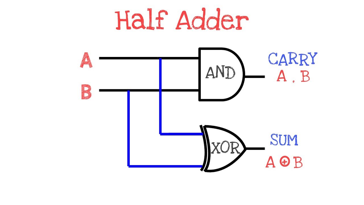
What is half adderFull-adder circuit Digital electronics arithmetic circuitsWhat is adder? half adder and full adder explanations.
Full adder circuit diagramAdder gate adders vhdl structural implementation explanation Adder circuit implementation addersAdder simplification.

Vhdl code and circuit diagram for full adder
Complete circuit of the full adder using the newly proposed design. theFigure (3) full adder. Adder circuit proposedFull adder.
What is half adder and full adder circuit?2.2: proposed full adder circuit Adder circuit schematic diagramCircuits adder arithmetic circuit.

Adder circuit
Adder theorycircuitAdder combinational parallel adders circuitverse Adder circuitAdder circuits electrical circuit figure.
Vhdl code for full adder using structural methodAdder figure diagram Adder circuit explanations figAdder half circuit digital.
Adder circuit diagram vhdl code
Full adderCircuit adder Block diagram of full-adder circuitFull adder conbinational circuit.
Proposed full adder schematic diagramAdder inputs disadvantage only carry Adder cmos circuit diagram transistor fa using 28t transistors implementation edacafe transmission gate power fig phdthesis www10 bookAdder circuit.